The promise of a global quantum internet has captivated researchers for decades. In theory, such a network would transmit information encoded in the quantum states of photons, enabling ultra-secure communication, distributed quantum computing, and entirely new forms of sensing. In practice, however, quantum communication has long been weighed down by an unglamorous reality: size.
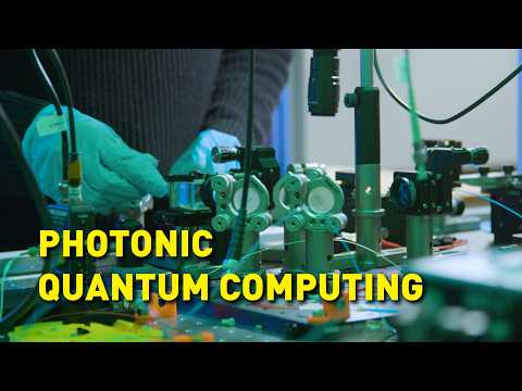
For years, quantum optics experiments required sprawling optical tables packed with mirrors, beam splitters, lenses, lasers, and stabilization hardware. These systems required painstaking alignment to sub-millimeter precision and were sufficiently fragile that slight vibration could disrupt an experiment. This “bulkiness problem” has been one of the biggest barriers preventing quantum networking from leaving the lab.
That barrier is now cracking—thanks to laser-written glass chips.
A quiet but profound transformation is underway in quantum photonics. Using femtosecond laser direct writing (FLDW), researchers can now “print” complex quantum circuits directly inside glass substrates. The result is a new class of devices that are compact, stable, and scalable, turning quantum communication from a tabletop experiment into something that looks increasingly deployable.
The Technology Behind the Shift: Femtosecond Laser Direct Writing
At the heart of this advance is the femtosecond laser: an ultrafast light source emitting pulses that last only a few quadrillionths of a second. These pulses deliver enormous peak power in an extremely localized region, allowing scientists to modify materials with surgical precision.
Unlike conventional chip fabrication, which relies on planar lithography, masks, and chemical etching, FLDW is a true three-dimensional manufacturing technique. It can add or modify structures deep inside a transparent material without disturbing the surface.
Here’s how it works:
- Focal precision: A tightly focused laser beam is directed into a transparent substrate such as fused silica or borosilicate glass.
- Refractive index modification: At the focal point, the laser’s energy permanently changes the glass’s refractive index.
- Waveguide creation: By moving the laser along a carefully programmed 3D path, researchers “write” waveguides—optical channels that trap and guide single photons.
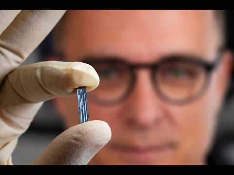
These waveguides function as microscopic conduits for light. Crucially, they can be arranged in complex three-dimensional geometries that are impossible to fabricate using traditional two-dimensional silicon processes. Helical arrays, multilayer interferometers, and densely interconnected networks can all fit into a chip no larger than a postage stamp.
This architectural freedom is transformative for quantum optics, where routing photons efficiently and reliably is essential.
Why Glass Is Emerging as the Quantum Substrate of Choice
Silicon has dominated classical computing for decades, but quantum communication imposes a different set of requirements. Glass, it turns out, checks many of the right boxes.
Low propagation loss is one of its biggest advantages. Photons traveling through glass waveguides experience minimal scattering and absorption, preserving fragile quantum states over longer distances. Recent advances in waveguide “composite morphology” have further reduced losses at bends, allowing for tighter routing and denser circuits.
Polarization stability is another critical factor. Many quantum protocols encode information in photon polarization, which is notoriously sensitive to imperfections. Glass-based photonic circuits can be engineered to be polarization-insensitive through thermal annealing, thereby helping to maintain quantum coherence as light propagates through the system.
Glass is also broadly transparent, spanning wavelengths from the visible spectrum to the telecom C-band around 1550 nm. That makes laser-written glass chips inherently compatible with today’s fiber-optic infrastructure—an essential requirement for any future quantum internet.
Finally, modern glass-ceramic materials offer exceptional thermal and mechanical stability. With ultra-low thermal expansion coefficients, these chips can operate reliably in fluctuating environments, including outdoor installations and even space-based platforms.
From Lab Curiosity to Field-Ready Hardware
Shrinking quantum photonics down to chip scale is not just an engineering milestone—it’s what makes real deployment possible. Over the past few years, several breakthroughs have pushed laser-written glass chips firmly into the “practical” category.
High-Fidelity Quantum Gates
Researchers have successfully integrated core quantum logic operations, including Hadamard and CNOT gates, directly onto glass chips. These gates are essential for generating Bell states—the benchmark of quantum entanglement. Reported fidelities approaching 99% meet the stringent thresholds required for reliable quantum communication.
Room-Temperature Detection
Historically, quantum photonics has often relied on cryogenically cooled detectors, thereby increasing cost and complexity. Recent demonstrations have shown direct coupling between laser-written glass circuits and silicon single-photon avalanche diode (SPAD) arrays that operate at or near room temperature. Achieving system-level detection efficiencies above 40% represents a major leap toward deployable systems.
Reconfigurable Photonic Circuits
Today’s glass chips are no longer static. By depositing thin metallic layers—often chromium and gold—onto the chip surface, researchers can create thermal phase shifters that dynamically alter optical paths. This reconfigurability enables a single device to perform multiple quantum communication or simulation tasks, thereby significantly improving flexibility and cost efficiency.
Toward a “Quantum-in-a-Box” Future
The long-term vision is deceptively simple: plug-and-play quantum networking hardware that works outside pristine laboratory conditions. Laser-written glass chips are emerging as leading candidates to realize that vision.
Because FLDW bypasses expensive semiconductor cleanrooms, these devices can be prototyped and manufactured more rapidly and at a lower cost. That scalability matters as quantum networks grow from isolated demonstrations into city-scale and eventually global infrastructure.
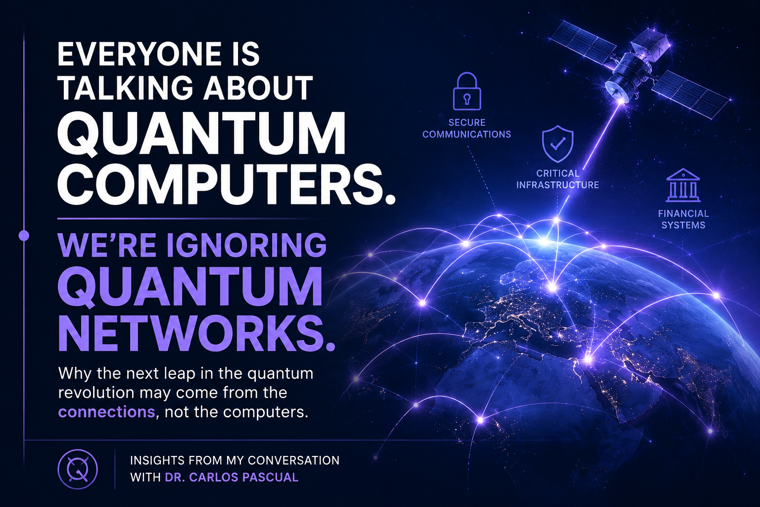
Looking ahead to 2026 and beyond, we are likely to see these chips embedded in Quantum Key Distribution (QKD) terminals, securing financial, governmental, and critical-infrastructure communications with physics-based encryption. What once required an entire optical table may soon fit inside a ruggedized box mounted on a building—or orbiting the Earth.
By collapsing complexity into glass, laser-written photonics does more than miniaturize hardware. It’s laying the structural backbone of the next internet, one photon at a time.